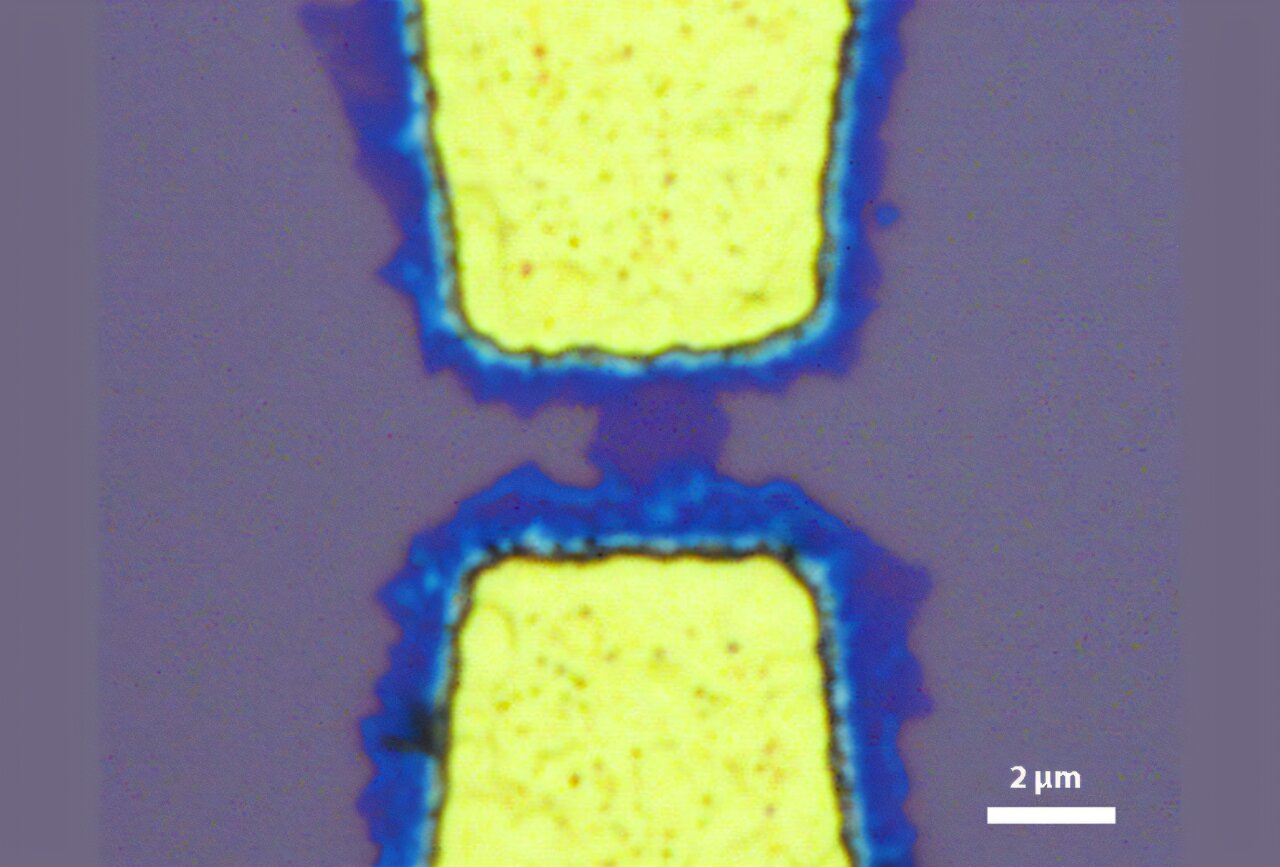

Transfer-Free Junction Obtained Via Chemical Vapor Deposation. Credit: Sathvik Iyengar / Rice University
A team of materials scientists at rice university have developed a new way to grow ultrathin semiconductor directly on too electronic components.
The method, described in a study Published in ACS Applied Electronic Materials, Could Help Streamline The Integration of Two-Dimensional Materials Into Next-Generation Electronics, Neuromorphic Computing and Other Technologies Demanding Ultrathin HIGH-Speed Speeductor.
The Researchers Used Chemical Vapor Deposation (CVD) to Grow Tungsten Dislenide, A 2D Semiconductor, Directly onto Patterned Gold Electrodes. They Next Demonstrated The Approach by Building A Functional, Proof-of-Concept Transistor. Unlike Conventional Techniques that Require Transferring Fragile 2D Films from One Surface to Another, The Rice Team’s Method Eliminates The Transfer Process Etilled.
“This is the first demonstration of a transfer-free method to grow 2D devices,” said Sathvik Ajay Iyengar, A Doctoral Student at Rice and a FIRST AITHOR ON THE STUDY ALONG MOTH RCE RCE RCE RCESTERAL AAHCE SATHORAL “This is a solid step toward Reducing Processing Temperatures and Making a Transfer-Free, 2D Semiconductor-Integration Process Possible.”
The discovery began with an unexpected observation during a routine experience.
“We received a sample from a collaborator that had gold markers patterned on it,” Sassi said. “DURING CVD Growth, The 2D Material Unexpectedly formed predominantly on the gold surface. Guide the growth of 2D semiconductors directly across them. “
Semiconductor are foundational to modern computing, and as the industry races toward smaller, faster and more Efficient components, Integrating Higher-Peerformance, Atomically Thin Materially Thin Materially Thin Materials LIK TUNGEN DISELENDE is a growing priority.
Conventional Device Fabrication Requires Growing The 2D SEMICONDUCTORE SEPARETELY, Usually at very high temperatures, then transferring it using a series of steps. While 2D Materials Promise to Outperform Silicon in Certain Metrics, Turning their lab-scale promise into industry industry-Relevant Applications have Proven Dificult-Proven Dificult -in Dificult –in Large Part Due to the FRAGIGITY OC Materials during the transfer process.
“The Transfer Process can degrade the material and damage its performance,” said Iyengar, who is part of Pulickel Ajayan’s Research Group at Rice.
The rice team optimized the precursor materials to lower the synthesis temperature of the 2D semiconductor and showed that it grows in a controlled, directional manner.
“Understanding how these 2D semiconductor interact with metals, especially when Grown in situ, is really valuable for future device fabrication and scality,” Said AJAYAN, RID AJAN, RID AJAYAN M. Greenwood Anderson Professor of Engineering and Professor of Materials Science and NanoenGineering.
Using Advanced Imaging and Chemical Analysis Tools, The team confirmed the method preserves the integrity of the metal contacts, which are vulnerable to damage at high temperatures.
“A lot of our work in this project was focused on proving that the materials system is stiff,” Iyengar said. “We are well-equipped here at rice to study the chemistry that goes on in this process to a very fine degree.
The success of the method lies in the strong interaction between the metal and the 2D material during Growing, Sassi Noted.
“The Absence of Reliable, Transfer-Free Methods for Growing 2D Semiconductors has been a major barrier to their integration into practical electronics,” He said. “This Workwal Unlock New Opportunities for Using Atomically Thin Materials in Next-Generation Transistors, Solar Cells and Other Electronic Technologies.”
In addition to challenges with the fabrication process, another key hurdle in 2D semiconductor design is electrical contacts’ quality, which entails not just low energy barriers but also stable and enduring Performance, scalability and compatibility with a wide range of materials.
“An-in-Situ Growth Approach Allows Us to Combine Several Strategies for Achieving Improved Contact Quality Simultaneously,” said anand anand puthirath, a co-corresponding author of the stuter Research Scientist at Rice.
The project was sparked by a question raised during a us-India research initiative: Could a Semiconductor Fabrication Process for 2D Materials be Developed on a Limited Budget?
“This Started Through Our Collection With Partners in India,” said Iyengar, who is a fellow of the japan social for the promotion of science and an inaugural recipe and an inaugural recipe Governments of the US, India, Australia and Japan to Support Early Career Scientists in Exploring How Science, Policy and Diplomacy Intersect on the Global Stage. “It showed how international partnerships can help identify practical constraints and inspire new approaches that work access global research environments.”
Togeether with a couple of his peers in the Quad Fellowship Cohort, Iyengar Co-Authored an article Advocating for “the need for expertise at the interaction of stem and diplomacy.”
“Greater Engagement Between Scientists and PolicyMakers is Critical to Ensure that Scientific Advancements Translate INTO Actionable Policies that Benefit Society as AS AS AS AS A.” “Materials Science is one of the areas of research where International Collection Cold Prove Invaluable, Especially Given Constraints Such as the Limited Supply of Critical Minerals and Supply Chain disruptions. “
More information:
Lucas M. Sassi et al, Mechanistic Understanding and Demonstration of Direct Chemical Vapor Deposation of Transition Metal Dichalcogenides Across Across Metal Contacts, ACS Applied Electronic Materials (2025). Doi: 10.1021/acsaelm.5c00828
Citation: Growing Ultrathin semiconductors directly on electric hts
This document is Subject to copyright. Apart from any Fair Dealing for the purpose of private study or research, no part may be reproduced without the written permission. The content is provided for information purposes only.