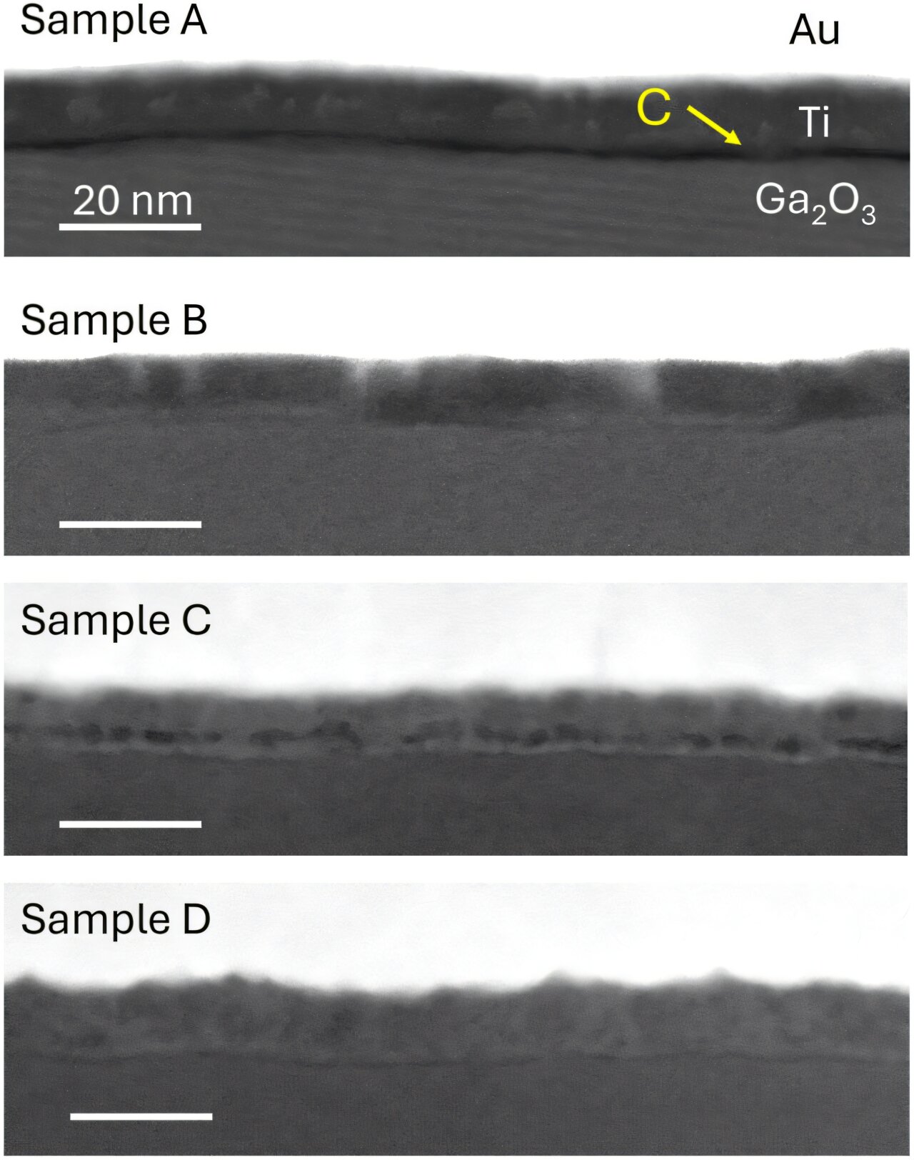
 Shows an ∼1 nm thick contamination layer between the ti and ga2o3 interface, which is not obsered in Linear Ohmic Contact Samples B-D. Credit: APL Materials (2025). Doi: 10.1063/5.0276786")
Overview of adf-company cross-sectional images of the metal contact au/ti/ga2O3 Interface. Sample A (Non-Conductive) Shows an ∼1 nm thick contamination layer between the ti and ga2O3 Interface, which is not observed in linear ohmic contact samples b -d. Credit: APL Materials (2025). Doi: 10.1063/5.0276786
Cornel Resarchers have Uncovered a Nearly Invisible Culprit Hindering The Development of Next-Generation, High-Power Electronics: A Microscopic Layer of Carbon CANTAMINATION, of Carbon Carbon Air Exposure and Fabrication Techniques, that Impairs Electrical Flow in Devices Made with Gallium Oxide. They have also found a solution.
A study Published June 20 in the Journal APL Materials Is Among the first to directly visualize this nanometer-thin barrier that can occur when metals are patterned onto semiconductors, an essential interface for Getting Current in and Out of Electronic Devices. When these contacts have resistance, device performance suffers.
The challenge is essaypatily pronounced in Beta Gallium Oxide, A Semiconductor Material with An utra-Band Gap That Cold One Day Allow Devices Like Electric VEHICLES and GRID InfRist Folding Efficiently Handle Higher Voltages.
“It’s been a problem in the Gallium oxide field for quite some time,” Said naomi pieczulewski, a doctoral student in materials Science and Engineering and the Study Author. “Sometimes you get good conduction and sometimes you get absolutely no conduction at all, and no one one should really Pinpoint who.”
Pieczulewski’s Research Spans Mulliple Cornel Labs Uniquely Positioned to Investigate The Problem, Including One Specializing in the Production of Oxide Materials and Oxide Materials and One Specializing in Antomic-Reportion Microscopy.
Focusing on the Interface Between a Beta Gallium Oxide and Titanium Contact, Pieczulewski and Colleagues Used Scanning Transmission Electron Electron Electron Microscopy and other Technique to Compare Two Common Methods for fabricating the contact: a traditional lift-off process, and a metal-friend process in which metal is deposited before the semiconductor is patterned.
, (c), (e), and (g) Atomic resolution adf-company images of the ti/ga2o3 interface along the [001] Zone Axis in Samples A -D. All Samples Show Ga Interstitial Columns Indicated by Yellow Arrows Near The Ga2o3 Surface. A Dark Contamination Layer Separates Ti from Ga2o3 in Sample A, While The Transition from Ga2o3 to Ti Results in Near -Per-Peerfect AdheRENCE in Samples B- D. Credit: APL Materials (2025). Doi: 10.1063/5.0276786")
(a), (c), (e), and (g) Atomic resolution adf-company images of the ti/ga2O3 Interface along the [001] Zone Axis in Samples A -D. All Samples Show Ga Interstitial Columns Indicated by Yellow Arrows Near The Ga2O3 Surface. A Dark Contamination Layer Separates Ti from Ga2O3 in sample a, while the transition from ga2O3 to ti results in near-Peerfect adherence in Samples B-D. Credit: APL Materials (2025). Doi: 10.1063/5.0276786
In the lift-off samples, the reserchers observed a thin, patchy layer of carbon between the metal and the semiconductor left over from photo photoresist Materials Used Dining Prose. To tackle the continue Beta Gallium Oxide Contacts.
Carbon Contamination Resulting from Air Exposure in the Metal-Fabrication Method was remedied with a five-minute active oxygen treatment, significantly lowering the contact resistance and impervowing Current flow.
“This research enables a way to produge reliable, consistent ultra-wide bandgap devices,” Pieczulewski said. “It’s an incremental program, but I think it’s significant in terms of moving towed commercialization.”
The Study’s Other Co-Lad Author is Kathleen Smith, Ph.D. ’24. Corresponding Authors Include Huili Grace Xing, The William L. Quackenbush Professor of Electrical and Computer Engineering and of Materials Science and Engineering; And David Muller, The Samuel B. Eckert professor of engineering in the school of applied and engineering physics.
The study was the first to unite on one research paper all set co-printigators of the Afrl-correct center for epitaxial solutions, also KNOWN AS AS ACCESS, Allied with Xing and Muller Include Debdeep Jena, The David E. Burr Professor of Engineering; Michael Thompson, The Dwight C. Baum Professor in Engineering; Darrell Schlom, The Tisch University Professor; Farhan Rana, The Joseph P. Ripley professor of engineering; And Hari Nair, Assistant Professor of Materials Science and Engineering.
Boise State University and Micron, Through the Semiconductor Research Corporation (SRC), Contributed Advanced Characterization Techniques to the Study.
More information:
Naomi Pieczulewski et al, Achieving 0.05 ω-mm contact resistance in non-alloyed ti/au ohmics to β-ga2O3 by removing surface carbon, APL Materials (2025). Doi: 10.1063/5.0276786
Citation: Researchers Identify Carbon Contamination as Key Barrier in Gallium Oxide Electronics (2025, July 28) Retrieved 28 july 2025 from https://techxplore.com/news/2025-07- carbon-contamination- key- barrier-gallium.html
This document is Subject to copyright. Apart from any Fair Dealing for the purpose of private study or research, no part may be reproduced without the written permission. The content is provided for information purposes only.